Single Board Relay Computer
Hacking the Verifone ZON Jr XL
Acoustic Delay Line Memory
Text Editor Performance Comparison
MPL
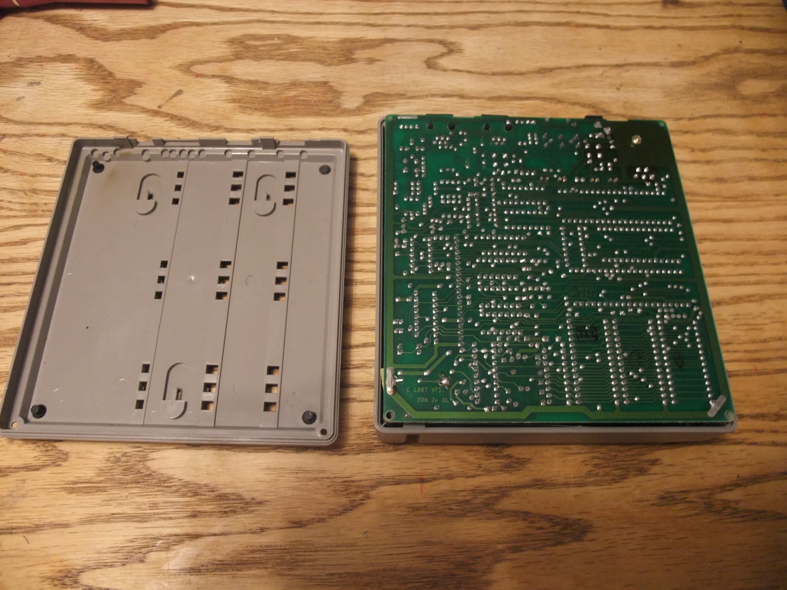
The Verifone ZON Jr XLLong ago I tried to start a business and wanted to accept credit card transactions, so I leased a credit card terminal from CardService International. The business went nowhere, but I leased this machine long enough so that eventually I came to own it. I'm sure it cost me at least $1500 in lease payments. It also has an 8-pin DIN connector on the back, I think for a printer: 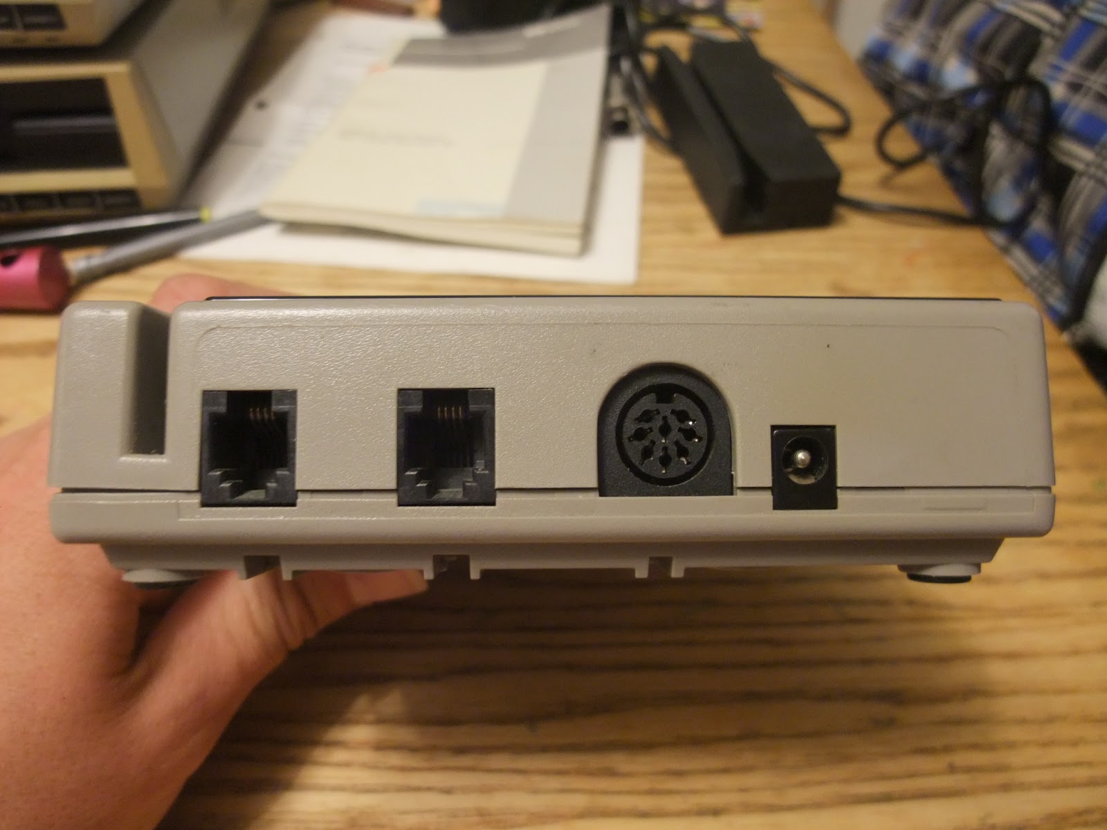 I'd better take it apart before I dump it... So what's inside of it?Two screws on the back remove the back cover:
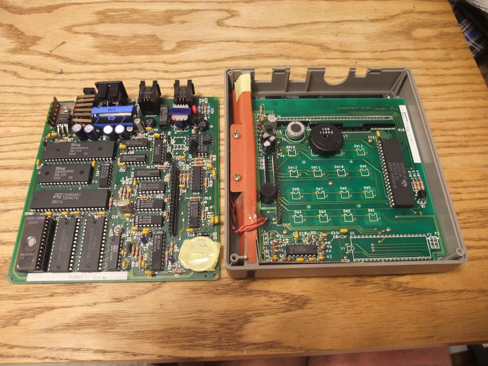
The circuit board can then be pulled straight up (no screws). There is a 20-pin SIP connector connecting the main board to a keypad/display board:
A close look at the main board and key/display board reveal 80's technology: all common through-hole chips:
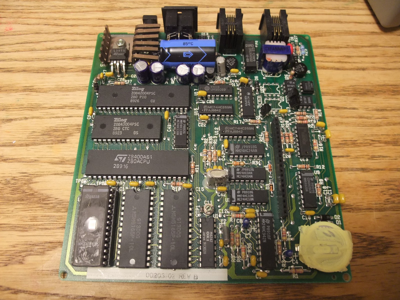
Reverse engineering is going to be easy! Parts ListSo what do we have? The main board has these chips:
Memory MapAn hour poking around with a continuity checker reveals the memory map. The 74HC10 and 74HC04 are used to make a simple address decoder for the memory space:
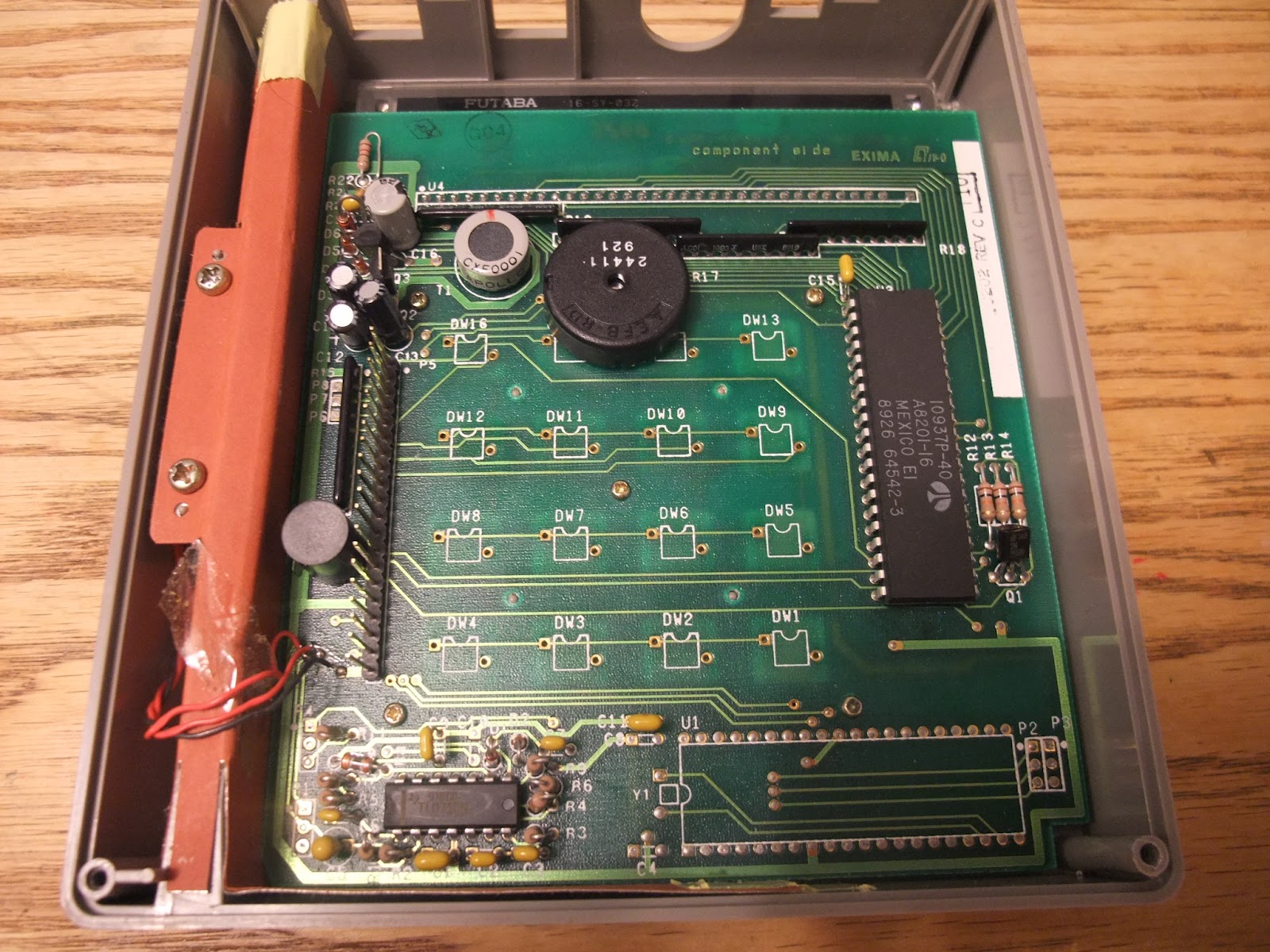
Sub-circuitsI should draw a schematic diagram for this thing, but it's so simple it's not really needed. Instead, here is a description of each of the sub-circuits I could find:SIP connectorHere is a pin-out of the SIP header which connects the main board to the keypad/display board. Pin one is the one closest to the back of the machine:
Power SupplyIt generates 5V and -5V with linear regulators. The -5V is used to power the negative rail of the OP-AMPs. The OP-AMP on the main board is used as a line driver for the data output pin of the DIN connector. The OP-AMP on the keypad/display board is the tape-head amplifier for the card reader.OscillatorOne half of the 74HC74 is used to divide the 7.15909 MHz oscillator (made with the crystal and some 74HC04 inverters) in half to make 3.579545 MHz for the main CPU clock and the touch-tone generator IC.ResetIt's provided by the L387A voltage regulator. It's connected to some chip select pins of the real time clock chip and the static RAM chips to help preserve their contents across reset. The static RAM chips and the real time clock chip are powered (through a diode-OR gate) by both line power and battery power.SpeakerThe piezo speaker is connected to the Q and ~Q outputs of second flip-flop in the 74HC74. The ~Q output is connected to the D input, so this flip-flop is wired up as a divide by two counter. The clock input is connected to the TO1 pin of the CTC: so you need to set up the CTC to generate the tone. The ~preset input is connected to the Q5 output of U12. I think the idea is to use this as an output enable bit so that you can leave the timer in the CTC always running.Serial PortA4 of the PIO is transmit data. B7 is receive data. I'm pretty sure that there was a schematic mistake with these assignments, since all of the other A pins are inputs and all of the other B pins are outputs. Anyway, the idea is that software needs to provide a "bit-banged" UART using these pins.These transmit and receive pins are connected to the CD4052 analog switch so that these same pins can be connected to different serial sources. The B and A address pins of the CD4052 are connected to U12 Q6 and Q7.
DIN connectorHere is the pin-out of the external connector:
KeypadU15 pins Q0 - Q3 drive the columns. A0 - A3 of the PIO are the row inputs.Touch Tone GeneratorB0 - B6 of the PIO are connected to the UM95089 touch tone generator chip. This chip is designed to be connected to a telephone keypad, so the software has to simulate a key-press by asserting one row bit and one column bit (by pulling the bits low, all of the others should remain high).DisplayTo write to the display, you just send one entire line of 16 character to it. Each character is sent as a byte in the range 0x00 - 0x3F, and the byte is serialized so that the MSB is sent first. A falling clock edge should be provided for each bit.From the datasheet, a reset pulse of at least 100 us needs to be provided. After reset, you must wait another 100 us before writing any data. The clock has a maximum high time of 20 us, so it must be kept normally low. The minimum pulse width is 1 us. After each byte transferred, you must wait 120 us. The brightness of the display is controlled with the duty cycle command: 0xC0 - 0xFF, where 0xC0 is off and 0xFF is brightest. The default brightness after reset is off, so we must send one of these commands to turn the display on. The column to start writing to can be controlled with the commands 0xA0 - 0xAF. The left-most column is 0xAF, next one is 0xA0, etc. This is the character set from the data sheet:  "Hello, world!" programWe now have enough information to write our own programs for this hardware.We could certainly write them in Z-80 assembly language, but there is a nice free C compiler available: the Small Device C Compiler: SDCC. Here is a program to write a message to the display: /* IoPorts for vacuum fluorescent display */ /* Note SDCC special directive to declare and locate IO ports */ __sfr __at 0x4a clr_clock; __sfr __at 0x4b set_clock; __sfr __at 0x4c clr_data; __sfr __at 0x4d set_data; __sfr __at 0x4e clr_reset; __sfr __at 0x4f set_reset; /* 7.54 us delay */ void delay() { /* Do nothing: the call / ret sequence is 7.54 us */ } /* At least 120 us */ void long_delay() { unsigned char x; for (x = 0; x != 20; ++x) delay(); } /* Serialize one byte and send it to display */ void send_byte(unsigned char c) { unsigned char scan = 0x80; do { if ((c & scan) != 0) { set_data = 1; } else { clr_data = 1; } set_clock = 1; delay(); clr_clock = 1; /* Falling edge when data is stable */ delay(); scan >>= 1; } while(scan != 0); long_delay(); /* 120 us delay after each character sent */ } /* Write entire line */ void send_msg(char *s) { char x; send_byte(0xAF); /* Point to first digit */ for (x = 0; x != 16; ++x) { if (*s != 0) { send_byte(0x3F & *s++); } else { send_byte(0x20); /* Spaces to end of line */ } } send_byte(0xFF); /* Enable display, full brightness */ } /* Initialize display */ void init_display() { clr_clock = 1; /* Clock is normally low */ clr_reset = 1; /* Assert reset */ long_delay(); set_reset = 1; /* Release reset */ long_delay(); } int main() { init_display(); send_msg("HELLO, WORLD!"); return 0; } To compile, we use the following command: sdcc -mz80 --xram-loc 0x8000 test.c The '-mz80' sets the architecture to Z-80. The '--xram-loc' sets the location of the RAM: the data section will be placed there. The compiler will link with an included simple C startup program, "crt0.s" and generate an Intel Hex Format file which can be used in the EPROM programmer. Crt0.s sets the stack to 0xFFFF and provides a jump instruction from the reset vector to the code. It places "reti" instructions in the interrupt vectors. If you have initialized global variables, they will be located in the data section (in RAM), and code will be generated to set their initial value. This code is located along with the rest of the code in EPROM.
The '@' at the end of the line is due to the fact that the ',' is not really a character: instead it turns out to be a modifier of the previous character. You can see that the ',' is not using an entire character position. So we intended to send 16 character, but really only sent 15, which left the last character left at its reset value. Anyway, my send_msg function needs to account for this. The '!' looks funny, but it's due to the font. |